Document Type : Original Article
Authors
- Imosobomeh Lucky Ikhioya 1, 2
- Nwamaka Ifeyinwa Akpu 3
- Edwin Uchenna Onoh 1, 4
- Samson Olatubosun Aisida 1, 2
- Ishaq Ahmad 2, 5
- Malik Maaza 6, 7
- Fabian Ifeanyichukwu Ezema 1, 8
1 Department of Physics and Astronomy, University of Nigeria, Nsukka, Nigeria
2 National Centre for Physics, Quaid-i-Azam University Campus, Islamabad, Pakistan
3 Department of Physics, Michael Okpara University of Agriculture, Umudike, Umuahia, Abia State, Nigeria
4 Department of Material Sciences, Addis Ababa University, Ethiopia
5 NPU-NCP Joint International Research Centre on Advanced Nanomaterials and Defects Engineering, Northwestern Polytechnical University, China
6 Nanosciences African Network, iThemba LABS-National Research, South Africa
7 UNESCO-UNISA Africa Chair in Nanosciences/Nanotechnology, College of Graduate Studies, University of South Africa, Muckleneuk Ridge, P.O. Box 392, Pretoria, South Africa
8 Africa Centre of Excellence for Sustainable Power and Energy Development, University of Nigeria, Nsukka, Nigeria
Abstract
In this research study, NiTe and NiTe/Mo were synthesized using an electrochemical deposition technique. The XRD spectrum displayed diffraction peaks at the (111), (200), (210), (211), (300), and (311) planes which corresponded to 13.22 o, 16.95 o, 18.85 o, 25.93 o, 30.84 o, and 32.98 o for NiTe and 13.41 o, 16.84 o, 18.85 o, 25.93 o, 30.84 o, 32.98 o for NiTe/Mo. The undoped film displays melted wax with oil splatter. The reaction between the transition metal and chalcogenide material is exposed by the nanoparticle. The film showed how the wax was transformed into stone-like nanoparticles at 40 oC. The U.V. area had the most absorbance and reflectance, yet transmittance grew as the wavelength grew. Adding molybdenum raised the precursor temperature, increasing the thickness from 132.02 to 150.21 nm and lowering the conductivity. Promising materials for solar devices are made possible by the synthesized materials' enhanced resistivity. A bandgap energy of 1.18 to 2.22 eV was discovered.
Graphical Abstract
)
Keywords
Introduction
Over the past two decades, transition metal chalcogenides have been a focus inmaterial science. Due to their variety of phases and stoichiometries, nickel has garnered the most interest, as well as the physical and chemical characteristics they display. Although nickel tellurides seem to have received less attention, most earlier works discuss research on NiS and, to a lesser extent, NiSe materials. A series of compounds are continuously produced between the chemical structures of nickel and tellurium, also known as NiTe. All stoichiometric nickel tellurides crystallize as hexagons, with the structures of NiTe being comparable to those of NiAs and Cd(OH)2. NiTe2 also forms a hexagonal crystal structure configuration between the crystal values of NiTe [1-3]. Nickel tellurides may be used various cutting-edge research domains, according to several recent studies. NiTe has been used as electrode materials in research on adenine and uric acid detection in supercapacitors, solar cell materials, physiological fluids, and glucose sensor anode materials for Li-ion batteries. The potential application of NiTe as electrocatalysts for oxygen/hydrogen evolution appears to be the most intriguing research topic [4]. Due to Te's lower electronegativity than S and Se's, which gives it ferromagnetic behavior and properties, tellurides appear more metallic. Tellurides perform better as electrocatalysts than sulphide and selenides. Utilizing substances that demonstrate photovoltaic application, a phenomenon researched in electrochemistry, physics, and photochemistry, photovoltaics (P.V.) converts light into electricity. Industry uses the photovoltaic material to make photosensors and generate electricity. The power system is managed by power electronics [5]. In a photovoltaic system, sun modules composed of several solar cells generate power. P.V. systems can be floating, fixed on walls, roofs, or the ground. The mount can either be permanently to track the sun as it moves across the sky, you may either fix it or use a solar tracker [6]. According to some, photovoltaic technology will be able to produce enough accessible, sustainable energy to decrease the consequences of CO2 global warming. As a source of energy, photovoltaic energy has several advantages. It does not emit any pollution or greenhouse gases once it is installed; in terms of power requirements, it is easily scaleable; and silicon is widely available in the Earth's crust, though other components needed by P.V. system manufacturers, such as silver, will eventually restrain further development in the technology [3-6].
In the past, the solid-state reaction used to make nickel tellurides was difficult for producing nano-sized products because it needed high temperatures, either an evacuated quartz ampule or an inert environment. Molecular precursor, solid-state metathesis, and telluride precipitation from aqueous solutions with unstable H2Te have been proposed. NiTe and NiTe2 thin films were recently produced through chemical vapor deposition and electrodeposition. Research is being done to create a better material platform. Metal telluride nanoparticles possess unique characteristics that make them adaptable and valuable across multiple scientific domains, including optics, electronics, magnetism, catalysis, biology, and thermoelectricity [7-9]. Transition metal chalcogenides have unique electrical properties, as multiple studies have revealed. These compounds comprise covalent bonds between chalcogens and transition metals [10]. Different transition metal chalcogenide phases have unique characteristics and uses. The oxidation states that occur most often in tellurium are -2, +2, +4, and +6 [11-15]. When the size decreases, especially when the radius reaches the Bohr radius, the conduction and valence bands are restricted to specific energy levels. Electrons in the bulk semiconductor material occupy stable excitation states at these levels. Due to their widespread usage in integrated circuit systems for multiple applications, metal telluride nanoparticles remain a highly significant technological component.
For semiconductor materials to be more commonly used in advanced devices, their structure, and therefore heat production, must align with particle size. Metal telluride semiconductor nanoparticles can be controlled to have a diameter of only a few nanometers by using the quantum confinement effect to create a broad range of energy bandgap visible regions [16]. GroupIV–VI nanomaterials have been studied for their potential application in FETs, infrared detectors, solar cells, and thermoelectric materials [17–20]. The oxidation potentials of tellurium compounds are lower than those of sulphur and selenium, with values of 0.60V and 0.95V, respectively. The energy bandgap is also relatively small at 1.51 eV [21]. The oxidation potential for these substances is lower, measuring 1.36 V and 1.85 V, with a corresponding energy bandgap of 1.71 eV. Cobalt telluride and nickel telluride were produced by Guo et al. [22]. They were used as counter electrodes to reduce I3 in dye-sensitized solar cells. NiTe2 counter electrodes produced photoelectric conversion efficiencies of 6.92% and 7.21%, which outperformed Pt-based ones in dye-sensitized solar cells. Telluride-based catalysts are effective in dye-sensitized solar cells. Metal tellurides have been synthesized using various methods, including PVD, solid-state metathesis, co-reduction, solvo (hydro)thermal, MOCVD, nonaqueous colloidal synthesis, microwave-assisted techniques, and electrodeposition [23-32]. Anand and Zaidan claim that there are no reports on NiTe thin films produced through electrodeposition because of the complexity of depositing a sufficient amount of Te into the film [27].
This study examines the structure and characteristics of NiTe/Mo films under the impact of precursor temperature. An easy and cost-effective electrochemical deposition technique was used to produce the films. Mo-dopant is effective because it can boost the free carriers by two electrons. The large valence difference between Mo+6 and Ni+2 ions promotes growth of Mo-doped NiTe thin films. The effect of Mo doping elements on the photovoltaic properties of NiTe thin films has not been studied.
Materials and Methods
Materials
Nickel telluride doped molybdenum (NiTe/Mo) was synthesized and characterized using the following materials: nickel chloride hexahydrate (NiCl2.6H2O), Molybdenum dioxide (MoO2), telluride dioxide (TeO2), Ammonia solution (NH3), distilled water, power source, Hydrogen Chloride (HCl), mantel heater, Multimeter, three-electrode cell arrangement with a potentiostat that delivers a D.C. voltage, a carbon electrode, fluorine-doped tin oxide as a substrate (FTO), thermostatic blast resettable oven with a temperature range of 50 °C to 1000 °C was used for annealing the grown films.
Substrate Cleaning Procedure
Substrates were soaked in methanol and washed with acetone and water. After a wash with distilled water, the substrates were kept for final oven drying.
Syntheses of NiTe and NiTe/Mo films
Three electrodes were used in the electrochemical deposition: a working electrode, a positive electrode of platinum mesh, and an Ag/AgCl reference electrode. The FTO, counter, and reference electrodes were inside the chamber in a row. NiTe and NiTe/Mo films were created at different precursor temperatures and pH levels using a potentiostat window with -200 mV versus a saturated calomel electrode for 5 s. 100 mL beaker measured the solvents. 10 V ran the deposition process. 10 mL of the diluted molybdenum precursor was added to the bath system. Table 1 outlines the gradual change of the material's molar concentrations required for the electrochemical bath setup. The samples underwent a 40-minute heating process at 350 oC to relieve their tension. The electrodeposition bath system includes distilled water, an anion source (Telluride dioxide for Te2-), a cation source (MoO2, NiCl2.6H2O for Mo2+, Ni2+), and a magnetic stirrer. The temperature was altered during the synthesis of nickel telluride-doped molybdenum films.
Table 1. Variations of Precursor's Temperature
Results and discussions
Resistivity and Conductivity Analysis
The electrical properties of NiTe and NiTe/Mo are shown in Table 2. When molybdenum was added, the precursor temperature was raised, increasing the thickness from 132.02 to 150.21 nm while also lowering the conductivity of the NiTe/Mo materials. The enhanced resistivity of synthesized materials enables the development of promising solar device materials. The relationship between film thickness and resistivity is illustrated in Figure 1-a, with resistivity increasing and conductivity decreasing as thickness increases [31]. Synthesized films are the preferred option for solar cells and photovoltaics applications. The graph in Figure 1b depicts the nonlinear pattern of resistivity and conductivity concerning precursor temperature, which shows their simultaneous increase and decrease.
Table 2. Displays the electrical characteristics of NiTe and NiTe/Mo materials

 Figure 1. In Figure 1, resistivity and conductivity are plotted against thickness and precursor temperature.
Structural Study
Figure 2 shows the X-ray diffractometer spectrum of NiTe and NiTe/Mo. The NiTe material is polycrystalline with a hexagonal structure. The XRD spectrum displayed diffraction peaks at the (111), (200), (210), (211), (300), and (311) planes which corresponded to 13.22 o, 16.95 o, 18.85 o, 25.93 o, 30.84 o, and 32.98 o for NiTe and 13.41 o, 16.84 o, 18.85 o, 25.93 o, 30.84 o, 32.98 o for NiTe/Mo. The undoped film displays melted wax with oil splatter. The action of the molybdenum dopant on the material deposited for photovoltaic application caused by the slight variation in the 2-theta angle of NiTe. Because of the dopant and precursor temperatures, the crystallinity of the films was also impacted. It was found that a rise in the precursor temperature caused the diffraction peak to rise, which increased the film's surface area for photovoltaic activities [32]. The structural values for the films are presented in Table 3. The films' grain sizes and lattice constant increased with the rise in precursor temperature. The new size would enhance the deposited films' crystallinity, which would also promote effective photon absorption. Applying Scherrer's relation in Equations 1-3, the structural values in Table 2 were determined for the regular grain size.
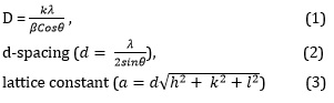
 Figure 2. XRD pattern of NiTe and NiTe/Mo @ a, Williamson-Hall plot @ b, Crystallite size against 2-theta angle @ c, and the plot of crystallite size and lattice strain against 2theta @ d
XRD results were used to draw the Williamson-Hall plot (β cos θ as a function Sin θ) shown in Figure 2b. The Williamson-Hall plot's slope rises with an increase in the antecedent temperature. The dislocation density increases with the precursor temperature, causing the crystallite size to change and the diffraction angle peak to grow due to strain hardening [33]. A plot of the deposit material's crystallite size as a function of the 2theta diffraction angle can be seen in Figure 2c. The NiTe material increased as the diffraction angle rose, unlike the precursor temperature-dependent change of the films. As the crystallite size grows, so does the diffraction angle. The specific position of the deformation of the films inside the diffraction angle was identified using the plot of crystallite size and lattice strain as a function of 2theta shown in Figure 2-d. Crystallite size increases with higher diffraction angles.
Table 3. Structural values for the deposited NiTe/Mo films


Figure 3. Surface morphology of NiTe @ (a); NiTe/Mo (40oC-50oC) @ (b-d)
Surface morphology of NiTe and NiTe/Mo temperature-dependent precursor synthesis
Figure 3 displays the surface morphology of NiTe and NiTe/Mo temperature-dependent precursor synthesis. Particles spread out on the films, allowing for even material deposition. The undoped film has a melted wax surface with oil splatters, and the nanoparticle reaction is transition metal and chalcogenide. The film melted at 40 oC showed how wax became stone-like nanoparticles. As a result, the films' stone-like nanoparticles were compressed as the precursor temperature increased. The material grain size of the films increased when the temperature reached 50 oC, making them suitable for light-emitting systems. Table 3 and Figure 2c show that the crystallite of the films develops with rising precursor temperature, except at 50 oC. Films created at lower temperatures suit solar cells and photovoltaic activity [34]. Figure 4 reveals the elemental analysis of the deposited films. The spectrum reveals fundamental elements, including nickel, telluride, and molybdenum. Undoped films have different compositions than doped films, as seen in Figure 4b. The substrate's constituent elements are additionally integrated into the syntheses.
 Figure 4. EDX spectrum of NiTe @ (a); and NiTe/Mo 40oC @ (b)
Optical study of NiTe and NiTe/Mo synthesized at different precursor temperatures
The absorbance, transmittance, and reflectance properties of NiTe and NiTe/Mo materials are showed in Figure 5. The U.V. area had the highest absorbance and reflectance, yet transmittance increased with the wavelength. The absorbance, transmittance, and reflectance of the films are enhanced by the dopant/precursor temperature. The temperature-dependent precursor affects NiTe-doped molybdenum's absorbance, transmittance, and reflectance. With an increase in temperature-dependent precursor, there was a decrease in absorbance due to nickel telluride-doped molybdenum. All deposited films absorbed light radiation in the visible and ultraviolet range, as shown by the spectra in Figure 1a. Lowering the temperature and dopant increases nickel telluride's absorption of U.V. light [34]. The absorption rate suggests the films are suitable for solar and photovoltaic cells. The films had a 90% or more transmittance for nickel telluride-doped molybdenum, 40% in ultraviolet, and 65% in near-infrared.
The high absorption caused a rapid decrease in nickel telluride transmittance. The spectra revealed that every film had a high level of transparency in both zones of Figure 5b. Adding this element to nickel telluride boosts its ability to transmit light when exposed to sunlight. The films that arise from synthesizing nickel telluride and nickel telluride-doped molybdenum have good transmittance, making them useful for solar and photovoltaic systems. Figure 5c illustrates the optical reflectance of NiTe and NiTe/Mo films. Its reflectance peaked in the U.V. region of the graph before dropping through both the visible and ultraviolet ranges [34]. The doped nickel telluride recorded over 20% in the UV region. The deposited films are suitable for solar and photovoltaic cells, as they have low reflectance values.
Figure 6 shows the band gap spectra of thin NiTe and NiTe/Mo films. The straight line on the plot of the coefficient of absorption squared against photon energy was extended to generate these spectra. A bandgap energy of 1.18 to 2.22 eV was discovered [34], according to the figure. As photon energy increases, the optical refractive index rises.

Figure 5. Absorbance @ (a); transmittance @ (b); and reflectance @ (c) against wavelength
 Figure 6. Energy band gap @ (a); and refractive index @ (b)
Conclusion
NiTe and NiTe/Mo have been synthesized successfully on the FTO substrate. At different precursor temperatures, the films were deposited. All the solutions used to deposit the thin films were prepared in distilled water. The growth of NiTe/Mo semiconductor thin film was affected by molybdenum. The XRD spectrum displayed diffraction peaks at the (111), (200), (210), (211), (300), and (311) planes which corresponded to 13.22 o, 16.95 o, 18.85 o, 25.93 o, 30.84 o, and 32.98 o for NiTe and 13.41 o, 16.84 o, 18.85 o, 25.93 o, 30.84 o, 32.98 o for NiTe/Mo. The molybdenum dopant caused a small change in the 2-theta angle of NiTe. Because of the dopant and precursor temperatures, the crystallinity of the films was also affected. The rising precursor temperature caused the diffraction peak to increase. This increased the film's surface area for photovoltaic activities. The film revealed melted wax and oil splatter. The nanoparticle reveals the reaction between metal and chalcogenide material. The film melted wax into stone-like nanoparticles at 40 oC. Maximum absorbance and reflectance were found in the U.V. area of the spectra. The absorbance, transmittance, and reflectance of the films are enhanced by the dopant/precursor temperature. The precursor temperature affects NiTe-doped molybdenum's absorbance, transmittance, and reflectance. Adding molybdenum raised the precursor temperature, increasing the thickness and reducing the conductivity. Promising materials for solar devices are made possible by the synthesized materials' enhanced resistivity. A bandgap energy of 1.18 to 2.22 eV was discovered.
Acknowledgments
Imosobomeh L. Ikhioya acknowledges the NCP-UNESCO-TWAS POSTDOCTORAL FELLOWSHIP FR number 3240325060 and appreciates the help of Prof. I. Ahmad and Prof. Ezema F. I. in making their study successful.
Disclosure Statement
No potential conflict of interest was reported by the authors.
Orcid
I.L. Ikhioya : 0000-0002-5959-4427
)