Document Type : Original Article
Authors
1 Department of Physics and Industrial Physics, Faculty of Physical Sciences, Nnamdi Azikiwe University, Awka, Nigeria
2 Department of Physics and Astronomy, Faculty of Physical Sciences, University of Nigeria, Nsukka, Enugu State, Nigeria
3 National Centre for Physics, Quaid-i-Azam University Campus, Islamabad, 44000, Pakistan
Abstract
In this research, zirconium was chosen as a dopant to improve the photovoltaic properties of lead selenide films. Using electrochemical deposition, we successfully deposited zirconium-doped lead selenide and undoped lead selenide films on FTO substrates. The X-ray diffraction pattern for the synthesized undoped and doped PbSe films shows a significant peak at the diffraction planes (220), (112), (310), (202), and (212) which confirm to the cubic structure with a preference orientation of the crystallites along the (202) plane. The Zr incorporation in the PbSe matrix opens up additional nucleation sites, inhibiting the formation of crystal grains and elevating the lattice strain, which may be the reason for the lower crystallinity in the PbSe/Zr films. With a thickness of 105.55nm, the undoped PbSe films were found to have resistivity and conductivity values of 6.20 x 10⁻⁵ (Ω.m) and 1.61 x 10⁻⁶ (S/m), respectively. When the Zr-dopant content was increased by 0.1 mol%, it was observed that the resistivity value climbed to 7.79 x 10⁻⁵ (Ω.m) and subsequently steadily decreased within the same range. The shrinkage of the PbSe/Zr films' grain size is responsible for the modest rise in resistivity. With a rise in Zr-dopant, the electrical conductivity falls from 1.61 x 10⁻⁶ (S/m) to 1.29 x 10⁻⁶ (S/m). An increase in the resistivity caused a drop in the conductivity. The bandgap for undoped PbSe is 1.10 eV. The bandgap was raised to 1.40–1.70 eV after adding Zr-dopant at a 0.1-04 mol% concentration.
Graphical Abstract
)
Keywords
Introduction
The advancement of science and technology is essential for creating novel materials. Creating high-quality materials is the primary aim of scientific advances and discoveries in materials [1,2]. Besides composition, other elements that affect material performance and features include the ability to adjust structure during syntheses. Semiconductors play a significant role in many technological applications. A better understanding of the characteristics of semiconductors has sped up technological development by enabling advancements in computer and electronics technology [3,4]. Semiconductors provide a variety of properties when placed on the surface of bulkier materials, making them electronic materials employed in the domains of optics, electronics, magnetics, chemistry, and mechanics. They can also be employed as components in electronic circuits since they respond differently from their volume properties when formed in a multilayer and behave as unique materials [5-10]. There are many ways to generate semiconductor materials, which are crucial to modern science and technology. Thin films' physical characteristics, such as their structural, morphological, optical, electrical, and magnetic properties, play a significant role in deciding the applications for which they are suitable [11-15]. It is crucial to thoroughly analyze the films' optical, surface, electrical, and structural features and the experimental techniques employed.
Studies have revealed that Lead Selenide, which can be employed as an absorber layer in solar cells, responds substantially more to bandgap and temperature variations than other semiconductor materials. Compared to other semiconductors, it is also quite sensitive to grain size. Due to these characteristics, lead selenide is frequently used to create nanostructured electronics [16-20]. There are many ways to create lead selenide films. Many techniques have been utilized to create lead selenide films, including microwave heating, SILAR, sputtering [12], spray pyrolysis, and chemical bath deposition [4-9, 17,18, 20-22]. Most of the above techniques are ineffective for low-temperature procedures, large surface coatings, and low manufacturing costs. It costs much money to cover vast regions with materials. Due to its low cost and simplicity of usage, the electrochemical deposition technique [10], which will be used in this work, is an intriguing technology for producing thin films. By adjusting the electric field, pH, and deposition durations, films can be deposited with this approach at density and thickness. It offers significant benefits, including simple film parameter control and application in a room environment with no complicated experimental setup [23-26].
Lead selenide films are created by Ravi and Chitra (2020) via chemical bath deposition over two hours at various temperatures. The polycrystalline structure of lead selenide films deposited at various temperatures may be seen in the XRD pattern. They discovered that the films had undergone a comprehensive purification process because the EDAX spectrum showed distinct peaks for Pb and Se but no other impurities [19]. Abeywickrama et al. [16] describe a two-step procedure for creating cubic lead selenide nanocrystals in the 20–40 nm size range. In particular, ~10 nm lead selenide QDs are made using the rapid injection technique, and the byproducts are then over-coated with more lead and selenium precursors. A study was conducted on using two lead reagents; lead oleate created cubes with a maximum size of 20 nm, whereas lead hexyl-decanoate, which is more reactive, produced noticeably larger nanomaterials with bulk bandgaps. Agglomerates were also visible in lead selenide films produced with lead hexyl-decanoate. Special care must be taken when X-ray powder diffraction is utilized to analyze more significant strained nanomaterials for which the Scherrer equation is insufficient. Congruent with electron microscopy characteristics [19]
To achieve high-quality semiconductor materials, doping is crucial. It is typically successful in regulating grain size, surface morphology, and crystal structure. As a result, doping lead selenide films with various elements can alter their optical, structural, magnetic, and electrical features [24,25]. There are many studies on lead selenide material doped with different elements, but it is still difficult for researchers to decide which doping elements to use and in what proportions to produce PbSe films of the highest quality.
In this research, zirconium was chosen as a dopant to improve the photovoltaic properties of lead selenide films. Using electrochemical deposition, we successfully deposited zirconium-doped lead selenide and undoped lead selenide films on FTO substrates. We considered how to lead selenide thin films' microstructural, morphological, and primarily optical characteristics were impacted by the quantity of zirconium doping. Compared to some of the physical features of the zirconium-doped lead selenide.
Experiments
Synthesis of PbSe and Zr-doped PbSe
The Zr-doped PbSe thin films were electrochemically deposited with fluorine-doped tin oxide (FTO) on glass slides. The FTO was first cleaned with acetone and methanol to prevent contamination and eliminate any imperfections from the substrates' surface. Following a distilled water rinse, it was placed in an airtight glass container. The chemicals used were of analytical grade reagent and were used without further purification to prepare all the solutions. Precursors included ammonia (NH3), lead (II) nitrate Pb(NO3)2, selenium (IV) oxide SeO2, zirconium (IV) oxide chloride, (Cl2Ozr.8H2O) and lead (II) nitrate (Pb(NO3)2 Selenium (IV) oxide (SeO2) and lead (II) nitrate Pb(NO3)2 were employed as sources for cation and anion, respectively. Zirconium (IV) oxide chloride octahydrate (Cl2Ozr.8H2O) was utilized as a dopant precursor. Ammonia (NH3) was used to adjust the pH of the reaction bath.
The PbSe/Zr aqueous electrolytic solution was prepared by measuring 20 mL of 0.1M of Pb(NO3)2 and 10 mL of 0.01M solution of SeO2 into a 100 mL beaker. The mixture was agitated using a magnetic stirrer for 5 min to obtain a homogeneous mixture. 0.01M solution of Cl2OZr8H2O, representing the dopant concentration, was measured into the same 100 mL beaker containing Pb(NO3)2 and SeO2. For many minutes, the entire mixture was swirled to ensure homogeneity. The dopant molarity of zirconium was varied as (0.1-0.4) mol% by adding 5 mL in each reaction precursor, while the pH and parameters were kept constant. In the reaction bath prepared, an FTO substrate and carbon electrode were connected to the DC power supply source for the electrochemical deposition process, and the room temperature was used for the deposition. Using a hand dryer, the substrates were taken out and dried. After deposition, the samples were subjected to annealing at 450 °C for 30 mins to remove stress on the surface of the films. The structural properties of the deposited PbSe/Zr films were identified using a multi-purpose X-ray diffractometer D8-Advance from Bruker that was operated in a continuous scan in locked coupled mode with Cu-Kα radiation (ʎ = 1.5406 Å)., In order to analyze the surface morphology of the films, scanning electron microscopy was performed. The 756S UV-Visible spectrophotometer was used to calculate the absorbance wavelength at 300 nm to 1100 nm at the optical spectral range. The optical spectral analysis of the absorbance values was used to infer the additional optical and solid-state features, and the Jandel four-point probes method was used to analyses the electrical properties of the films.
Result and Discussion
Structural properties of undoped PbSe and Zr/PbSe films at a dopant concentration
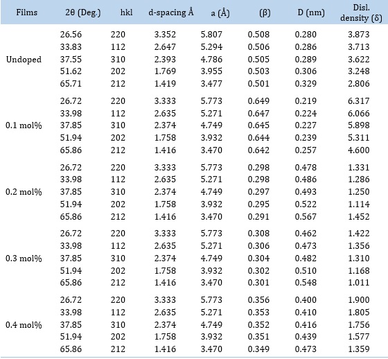
Figure 1 (Z1) displays the X-ray diffraction pattern for the generated undoped PbSe and PbSe/Zr films at various dopant concentrations. The significant observed peaks for the PbSe/Zr and undoped PbSe films are located in the diffraction planes (220), (112), (310), (202), and (212). These confirm that all deposited films (undoped PbSe and Zr doped PbSe) crystallize well in the cubic structure with a preference for orientation of the crystallites along the (202) direction. They are equivalent to the JCPDS card: 01-076-1799. Lower crystallinity for the PbSe/Zr films is indicated by the diffraction peaks' reduced intensities compared to the undoped PbSe film. The Zr incorporation in the PbSe matrix opens up additional nucleation sites, inhibiting the formation of crystal grains and elevating the lattice strain, which may be the reason for the lower crystallinity in the PbSe/Zr films [4, 10-12] have noted comparable tendencies. With the addition of the Zr dopant to the undoped PbSe film, the level of sharpness of the diffraction peaks likewise falls.
The additional structural characteristics, including crystallite size, dislocation density, and lattice constants, are reported in Table 1. The table showed that adding the Zr dopant causes the crystallite size to grow. This could be due to increased nucleation center densities in the doped films, leading to enhanced crystallite development [4, 10-12]. The Zr dopant ranged from 0.1 mol% to 0.4 mol%, and the crystallite size was between (0.219-0.410) nm. Except for the 0.2 mol% films, which recorded a dislocation density value lower than that of the undoped PbSe film, it was discovered that the dislocation densities increased with Zr doping. It was discovered that Zr doping caused a drop in the lattice constant values. It was found that the slope of the Williamson-Hall plots, which are shown in Figure 1 (Z2), increases as the dopant concentration increases. The crystallite size varies as the dopant concentration increases, the dislocation density increases, and strain hardening causes the prominent peak of the diffraction angle to grow. Figure 1 (Z3) plots the deposited material's grain size against 2-theta. The plot showed that the material fluctuated as the 2theta increased, in contrast to the dopant concentration-dependent variation of the material. The size of the crystallite causes an increase in the diffraction angle.
 Figure 1. Synthesis plan and surface modification of magnetic nanocomposites with cisplatin
Table 1. Structural values of PbSe and PbSe/Zr films
The electrical resistivity and conductivity of PbSe and PbSe/Zr
The four-point arrangement, which measures the corresponding current values for each voltage applied across the film, was used to evaluate the electrical resistivity and conductivity of PbSe and PbSe/Zr films with various variations. The silver paste was used to guarantee ohmic contact with the film. The electrical characteristics of PbSe and PbSe/Zr at various Zr-dopant concentrations are presented in Table 2. With a thickness of 105.55 nm, the undoped PbSe films were found to have resistivity and conductivity values of 6.20 x 10⁻⁵ (Ω.m) and 1.61 x 10⁻⁶ (S/m), respectively. When the Zr-dopant content was increased by 0.1 mol%, it was observed that the resistivity value climbed to 7.79 x 10⁻⁵ (Ω.m) and subsequently steadily decreased within the same range. The shrinkage of the PbSe/Zr films' grain size is responsible for the modest rise in resistivity [4, 10-12]. With a rise in Zr-dopant, the electrical conductivity falls from 1.61 x 10⁻⁶ (S/m) to 1.29 x 10⁻⁶ (S/m). An increase in the resistivity caused a drop in the conductivity.
PbSe/Zr resistivity and conductivity as a function of thickness are plotted in Figure 2 (Z4) for various dopant concentrations. It was discovered that the growth in the films' resistivity and conductivity impacted their thickness. Figure 2 (Z5) shows the plots of resistivity and conductivity vs. Zr-dopant concentration and demonstrates that an increase in Zr-dopant concentration led to an increase in the resistivity and conductivity of the synthesized film. The plot of dopant concentration vs. film thickness is presented in Figure 2 (Z6), and it demonstrates that both the dopant and the film thickness have a commensurate increase, with the maximum film thickness being 108.42 nm or 0.4 mol% of Zr-dopant. This may be explained by the fact that the number of solute particles in the solution deposited onto the substrate increases with dopant concentration.
Table 2. Electrical properties of PbSe and PbSe/Zr

 Figure 2. resistivity and conductivity vs. Thickness (Z4), dopant molarity of zirconium (Z5), and dopant molarity vs. Thickness (Z6)
Optical properties of PbSe and PbSe/Zr
Figure 3 (Z7) displays the optical absorbance spectra of undoped PbSe and PbSe/Zr films at various dopant concentrations. The undoped PbSe maintains a constant absorbance value throughout the UV-Vis and NIR spectrums. After adding 0.1 mol% of Zr dopant, the absorbance of the films rose in the UV-Vis region of the spectrum. A dramatic increase in absorbance value in the UV-Vis region was triggered by a further increase in the Zr dopant concentration to 0.2 mol%. As the Zr dopant concentration rose to 0.4 mol%, it was found that absorbance values that were lower than those of undoped PbSe began to decrease. This demonstrated that Zr doping enhanced the PbSe film's ability to absorb light spectrum [4, 10-12], making it suitable for solar photovoltaic applications. The synthesized films' transmittance is shown in Figure 3 (Z8); the undoped films' transmittance steadily rises from the UV to the NIN spectral regions. As the dopant concentration grows, the number of Zr-doped films increases, demonstrating how Zr-dopant affects the production of films for photovoltaic use. The reflectance spectra of the undoped PbSe and PbSe/Zr films at various dopant concentrations are shown in Figure 3 (Z9). The reflectance of the undoped PbSe film was low in the UV region and gradually increased toward the NIR region. When 0.1 mol % of Zr-dopant is added, reflectance values in the NIR region sharply rise above those of the PbSe film that is not doped. The reflectance value in the visible region increased sharply when the Zr-dopant concentration was raised to 0.3 and 0.4 mol%, respectively, then progressively decreased toward the NIR region to a level lower than that of the undoped PbSe film. The reflectance values of all the Zr-doped PbSe films were higher than those of the undoped PbSe films. The bandgap graphs for undoped and PbSe/Zr films at various dopant concentrations are shown in Figure 3 (Z10). By extrapolating the straight portion of the absorption coefficient square against the photon energy to the photon energy axis, the optical bandgap of the films was found. It has been determined that the bandgap for undoped PbSe is 1.10 eV. The bandgap was raised to 1.40 eV after Zr-dopant was added at a concentration of 0.1mol%. After then, the bandgap increased to 1.50 eV at 0.2 mol% Zr-dopant. A bandgap value of 1.60 eV is produced by increasing the Zr-dopant concentration by one more time to 0.3 mol%. Zr-dopant at 0.4 mol% produced a bandgap value of 1.70 eV.
The plot of the refractive index Vs. photon energy for undoped PbSe and PbSe/Zr films at various dopant concentrations is shown in Figure 4 (Z11). As the photon energy rose, the refractive index value of the undoped PbSe film slowly decreased. As the photon energy rose, the refractive index values in the PbSe/Zr films showed a significant decline. Except for 0.4 mol% of Zr-dopant, which has a refractive index value higher than that of the undoped PbSe film, all PbSe/Zr films produced lower values of the refractive index due to Zr doping. Figure 4 (Z12) demonstrates that when the photon energy rose, the extinction coefficient value for the undoped PbSe films continued to drop steadily. As the photon energy increased, the introduction of Zr-dopant caused a rise in extinction values. Zr-dopants at concentrations of 0.1, 0.2, and 0.3 mol% exhibits greater extinction coefficient values than undoped PbSe [4, 10-12]. An extinction coefficient value lower than undoped PbSe was obtained by increasing the Zr-dopant concentration to 0.1mol%. According to Figure 4 (Z12), the optical conductivity value of the undoped PbSe film steadily increased as photon energy increased. For 0.1mol%, 0.2mol%, and 0.3mol% of Zr, optical conductivity values first rise sharply due to the Zr-dopant before falling below those of the undoped PbSe films. Zr at 0.4 mol% produced an optical conductivity value lower than undoped PbSe.
Figure 5 (Z14) demonstrated that when the photon energy increased, the real dielectric constant for the undoped PbSe film remained constant. Except for 0.4 mol% of Zr, which produced a more excellent real dielectric constant value, the introduction of Zr-dopant first causes a rise in the value of the real dielectric constant, which eventually declines to a level below that of undoped PbSe [4, 10-12]. As seen in Figure 5 (Z15), adding Zr dopant reduces the values of the imaginary dielectric constant of the undoped PbSe film.
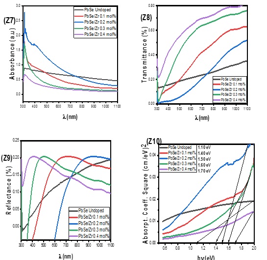
Figure 3. Absorbance (Z7), transmittance (Z8), reflectance (Z9), and bandgap (Z10)
 Figure 4. Refractive index (Z11), extinction coefficient (Z12), and optical conductivity (Z13)
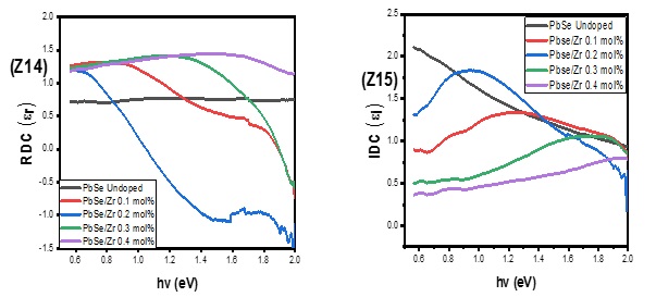
Figure 5. Real (Z14), and imaginary (Z15) dielectric constant
Surface morphology of PbSe and PbSe/Zr
Figure 6 (Z16) displays the SEM micrograph of the undoped PbSe film. The morphology showed that the surface of the undoped PbSe film has more randomly spaced nanocrystalline grains. On the surface of the FTO, the micrograph revealed a homogeneous distribution of hollow, spherical nanosized granules. The surface grains coalesce into a well-pack size of the rove-like structure at 0.1–0.2 mol% (Z17-Z18) Zr dopant, which is denser than the undoped PbSe film. The surface displays a less tightly packed, nearly uniform distribution of nanocrystalline grains at 0.3–4 mol% (Z19-Z20) Zr dopant. As the Zr dopant concentration rises, the surface morphologies of the Zr-doped films become less densely packed. The long chains of grains and strongly defined grain boundaries found in the synthesized PbSe/Zr films generally demonstrate structural homogeneity [24,25]. The porosity of the synthesized materials increased high charge transport resistance by lowering particle-particle interconductivity and raising grain boundary density [26].
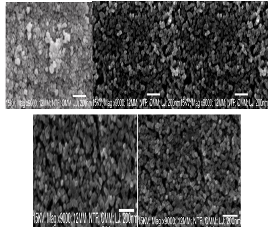
Figure 6. Surface morphology of PbSe (Z16) and PbSe/Zr (Z17-20)
Conclusion
PbSe and PbSe/Zr have been synthesized using electrochemical deposition and FTO as the substrate. The X-ray diffraction pattern confirms a cubic structure with a (202) plane orientation. Zr incorporation in the PbSe matrix inhibits crystal grain formation. With a thickness of 105.55 nm, the undoped PbSe films were found to have resistivity and conductivity values of 6.20 x 10⁻⁵ (Ω.m) and 1.61 x 10⁻⁶ (S/m), respectively. The resistivity value rose to 7.79 x 10⁻⁵ (Ω.m) when the Zr-dopant content was increased by 0.1 mol%, then decreased. The shrinkage of the PbSe/Zr films' grain size handles the modest rise in resistivity. With a rise in Zr-dopant, the electrical conductivity falls from 1.61 x 10⁻⁶ (S/m) to 1.29 x 10⁻⁶ (S/m). An increase in the resistivity caused a drop in the conductivity. The bandgap for undoped PbSe is 1.10 eV. After adding Zr-dopant at a 0.1-04 mol% concentration, the bandgap increased to 1.40-1.70 eV. The undoped PbSe maintains a constant absorbance value throughout the UV-Vis and NIR spectrums. After adding 0.1 mol% of Zr dopant, the absorbance of the films rose in the UV-Vis region of the spectrum. A dramatic increase in absorbance value in the UV-Vis region was triggered by a further increase in the Zr dopant concentration to 0.2 mol%.
Disclosure Statement
No potential conflict of interest was reported by the authors.
Orcid
I.L. Ikhioya : 0000-0002-5959-4427
)